Graphene
- A single layer of carbon atoms in a hexagonal honeycomb lattice: one atom thick, a true 2D material.
- High electrical conductivity and high carrier mobility.
- Zero band gap: the valence and conduction bands meet at the Dirac point, so graphene conducts with both electrons and holes.
- Highly thermally conductive, mechanically strong, and flexible.
- Large surface-to-volume ratio.
The graphene field-effect transistor
- Graphene forms the conductive channel between the source and drain electrodes.
- A small, fixed source–drain voltage (Vds) drives a current (Ids) through the channel.
- The side-gate electrode sits on the same chip surface as the channel instead of underneath it like a conventional back gate. Back-gated devices also work, but side-gated devices are preferred for biosensors because they're more sensitive.
- The graphene channel and side gate are both exposed to a liquid ionic electrolyte.
- A gate voltage (Vg) is applied between the side gate and the graphene and swept over a set range.
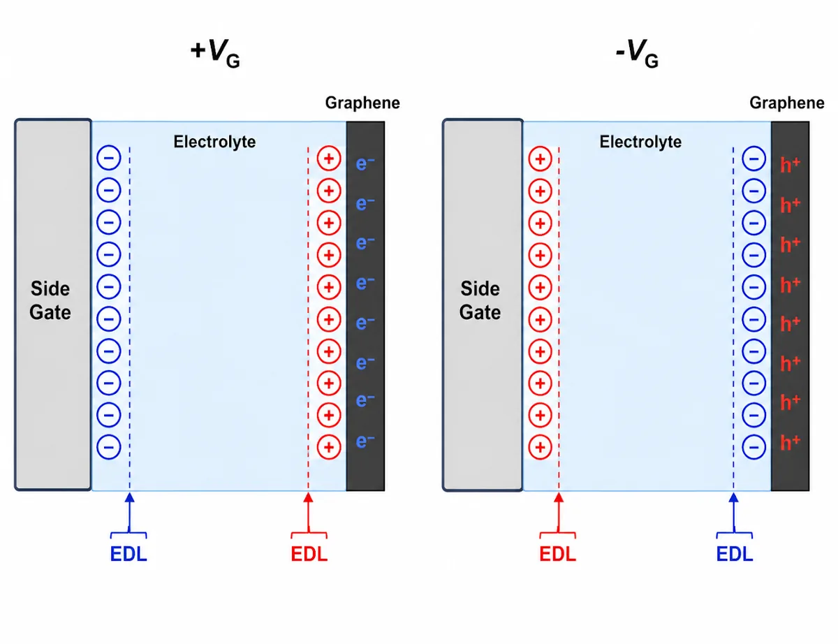
- The electrolyte lets the gate voltage create an electric field at the graphene–electrolyte interface. Ions rearrange into an electric double layer (EDL), which behaves like a very thin capacitor.
- That field shifts graphene's Fermi level and carrier concentration. On one side of the Dirac point conduction is hole-dominated (p-type), on the other it's electron-dominated (n-type).
- While Vg is swept, Ids is measured at roughly constant Vds. Plotting Ids against Vg gives the transfer curve.
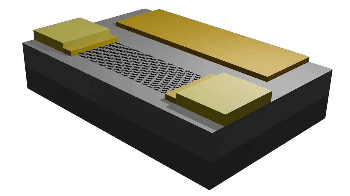
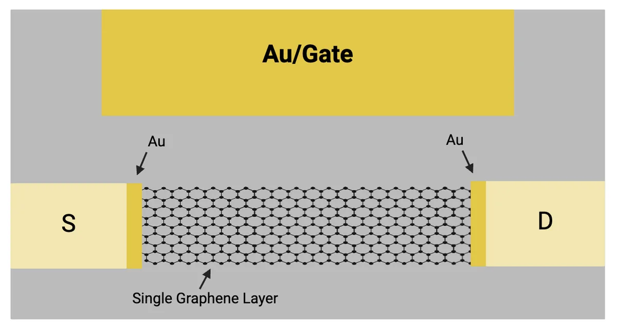
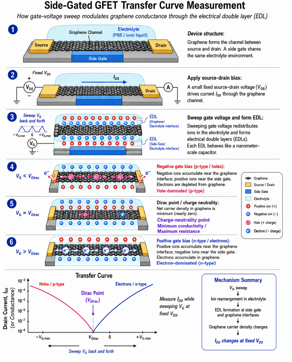
Side-gate GFET overview
- Source–drain bias: a small fixed voltage drives current through the graphene channel from source to drain.
- Gate voltage sweep: sweeping the side gate builds electric double layers whose polarity follows the gate.
- Negative gate bias gives hole conduction, on the left of the Dirac point.
- At the Dirac (charge-neutrality) point, resistance is at its maximum.
- Positive gate bias gives electron conduction, on the right of the Dirac point.
Example: applying a positive Vg
- A positive gate voltage is applied relative to the graphene, creating a potential difference between the side gate and the channel.
- Ions in the electrolyte rearrange. Anions move toward the positive gate, and cations gather near the graphene.
- The cation layer near the graphene forms an EDL with the graphene surface.
- Because the graphene is connected to the source and drain, electrons flow from the contacts into it, forming the negative charge opposite the ionic layer.
- Electrons accumulate until the electrostatic forces reach equilibrium. The graphene now has a higher electron density and becomes n-type.
- The fixed Vds drives these electrons through the channel, producing the measured Ids.
The Dirac point
The Dirac point is the gate voltage where:
- ne = nh (electron and hole densities are equal).
- Net carrier density is near its minimum, so conductivity is at a minimum and resistance at a maximum.
A typical transfer curve runs from hole conduction, through the Dirac point, to electron conduction. The gate voltage electrostatically changes graphene's carrier concentration and conductivity, and graphene's zero band gap allows continuous ambipolar conduction.
The Dirac point is the gate voltage at which graphene approaches charge neutrality: minimum carrier concentration, minimum conductivity, and maximum channel resistance.
Electric double layer (EDL)
- When positive or negative ions gather near the graphene channel, the neutral graphene has to supply the opposite charge, forming the EDL. Positive and negative charge must balance.
- The source and drain electrodes act as electron reservoirs.
- Depending on the polarity of the ions that gather, the graphene sends electrons to the electrodes or receives them:
- Sending electrons leaves an electron deficiency, giving hole conduction.
- Receiving electrons makes electrons dominate, giving electron conduction.
- The opposite charges induced by electrolyte ions near the graphene set whether conduction is p-type or n-type.
How gate voltage controls conductance
- Vg creates an electric field across the graphene–electrolyte interface that adds or removes charge carriers.
- Vg changes graphene's electrostatic potential and shifts its Fermi level:
- More negative Vg gives more holes (p-type), so conductance rises.
- At the Dirac point there are minimum carriers, so conductance falls.
- More positive Vg gives more electrons (n-type), so conductance rises again.
- The result is the characteristic V-shaped transfer curve.
As a biosensor
Molecules on the graphene channel
- DDT attaches to the Au gate through its thiol group to stabilize it.
- PBASE links the graphene to the DNA aptamers.
- DNA aptamer binds a specific target molecule and folds. The folded and unfolded states apply different electric fields to the graphene, shifting its Dirac point.
- Ethanolamine (ETA) passivates PBASE that has no aptamer, preventing unwanted binding.
How a test works
- Sweat samples are collected from the patient.
- The sample is dropped onto the graphene channel.
- The Dirac voltage is compared against the baseline to confirm the aptamer–target binding event.
- The result indicates whether the marker is present, similar in purpose to a COVID test kit but with a different mechanism.