Process traveler
Each step links to a full write-up with parameters, recipe, mechanism, and tool anatomy.
| # | Process | Tool | Write-up |
|---|---|---|---|
| 01 | Substrate clean (SC-1 / RCA-1) | Wet bench | Substrate preparation |
| 02 | Resist coat and develop | AZ 1529, LOR5B / AZ 1518, AZ MIF 300 | Photoresist and surface profile |
| 03 | Lithography | Heidelberg MLA | Photolithography |
| 04 | Cr/Au contacts and lift-off | Temescal BJD-1800 e-beam | E-beam evaporation and lift-off |
| 05 | SiO₂ passivation | Oxford PlasmaLab PECVD | PECVD oxide passivation |
| 06 | SiO₂ etch | Trion ICP-RIE | Reactive ion etching |
After these steps come graphene transfer (APS Cu etch with PMMA support), wire bonding to a custom PCB, and electrical testing on a probe station.
Failure modes and solutions
Two fabrication problems I diagnosed and fixed while building back-gated GFETs.
Failure mode 1: Resist edge bead
ProblemAn edge bead raised the wafer edge, so the maskless aligner couldn't find focus and patterns came out misaligned.
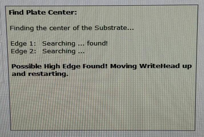
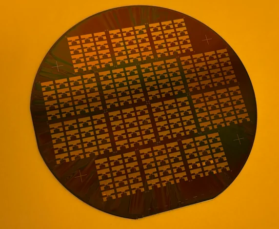
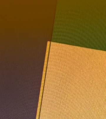
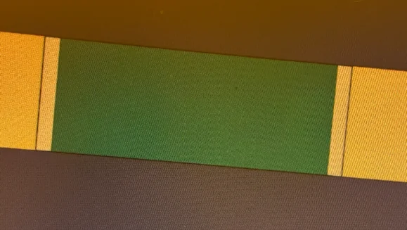
FixA two-step spin coat (slow spread, then fast spin to target thickness), followed by edge-resist removal with acetone, then IPA.
ResultThe aligner focused normally and patterns were well aligned after development (d).
Failure mode 2: Resist residue after graphene transfer
ProblemThick single-layer AZ 1529 couldn't be stripped cleanly from the graphene channel, and sonication wasn't an option because it damages graphene.
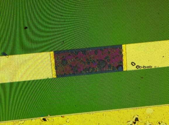
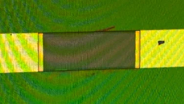
FixSwitched to an LOR5B / AZ 1518 bilayer. The LOR undercut lets the stack lift away in PG Remover without sonication.
ResultComplete resist removal after graphene patterning, with no visible residue in the channel (b).
Equipment I operate
- Photoresist spin coating (AZ positive photoresist series)
- Maskless lithography (Heidelberg MLA)
- Photoresist development (AZ MIF 300)
- Reactive ion etching (Trion ICP-RIE)
- E-beam evaporation (Temescal)
- Plasma-enhanced CVD (Oxford PlasmaLab)
- Atomic layer deposition (Beneq ALD)
- Surface profilometry (Bruker Dektak XT surface profiler)
- Wet etching (Cu foil etching in ammonium persulfate)