NanoEngineering · UC San Diego

Youngjun
Kweon

I build graphene FET biosensors in the Nano3 cleanroom, from bare silicon to wire-bonded die.

Résumé (PDF) LinkedIn ↗
1+ yrNano3 cleanroom user
Top 8 of 25TSMC-UCSD Academy, 300+ applicants
9 stepsGFET process flow, wafer to package
3.646GPA, B.S. expected 2028
About

Junior in NanoEngineering at UC San Diego

Youngjun Kweon

I'm a third-year B.S. NanoEngineering student in the Department of Chemical and Nano Engineering at UC San Diego. My work sits where semiconductor processing meets sensing: I fabricate graphene field-effect transistors in the cleanroom and use them to detect hormones in sweat at picomolar levels.

I've run the full process flow myself, from SC-1 cleaning and maskless lithography through e-beam evaporation, PECVD, and reactive ion etching to wire bonding and probe-station testing. This site documents each step, the physics behind the device, and the study notes I keep on semiconductor fabrication.

I'm looking for internships in semiconductor process engineering, device fabrication, and biosensing.
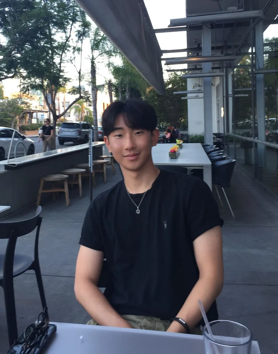
Now · Fall 2026

Two new programs this quarter

Both started in November 2026 and build directly on my cleanroom work.

Selective program

TSMC-UCSD Academy

Nov 2026 – Jun 2027

  • Selected as one of the top 8 students in a 25-member cohort chosen from more than 300 applicants by TSMC and UCSD review committees.
  • Training on industry-oriented microfabrication processes and equipment in Nano3.
  • Next: leading a semiconductor process development project with UCSD faculty.
Paid research internship

Galiana Technology

Nov 2026 – Present · via CMRR, UC San Diego

  • Supporting fabrication of Nanofids, a BCI device that detects neuron activation, as it shrinks toward 20 µm³.
  • Developing an architecture that combines a PV panel, quantum wells, and a calcium FET switch in one device.
Research

Graphene devices for sensing

Two labs, one device platform. In the Lal Lab I use GFETs to detect hormones. In the Vazquez Mena Lab I add quantum dots to give them an optical sensing mode.

Jul 2025 – Present

Biosensor Fabrication and Testing

Prof. Ratnesh Lal Lab

Manuscript under review · GFET detection of estradiol and cortisol
Read the project write-up →
  • Ran aptamer-functionalized GFET sensing for label-free estradiol and cortisol detection in PBS and artificial sweat.
  • Measured transfer curves (Ids–Vgs) on a probe station and tracked Dirac-point shifts across pM–nM concentrations.
  • Analyzed dose-response, sensitivity, repeatability, and selectivity against interfering steroid hormones in Python and Excel.
  • Wrote sections and prepared figures for the manuscript.
Jul 2025 – Present

Materials and Optoelectronics

Prof. Oscar Vazquez Mena Lab

About this lab →
  • Fabricated CdSe quantum-dot structures to integrate with graphene devices as an optical sensing modality.
  • Optimized graphene transfer (APS Cu etch), PMMA removal, and annealing to improve GFET response and repeatability.
  • Tracked electrical changes after each step (transfer, anneal, QD deposition, illumination) to isolate process effects.
  • Ran photoluminescence on CdSe/graphene/biomolecule stacks and designed GFET layouts and process flows.
Explainer

GFET Device Physics

How the sensor works

Read the explainer →

Side-gated GFET operation, the Dirac point, the electric double layer, and how aptamer binding turns into a measurable voltage shift.

Process traveler

How I build a GFET

The fabrication sequence I run in the UCSD Nano3 cleanroom. Each linked step has its own write-up with the recipe and the physics behind it.

StepProcessTool / recipePurpose
01Substrate cleanSC-1 · DIW:NH₄OH:H₂O₂ 5:1:1Remove organics and particles from (100) Si wafers.
02Resist coatAZ1529 · LOR5B/AZ1518 bilayerSingle layer for oxide etch; bilayer gives an undercut for lift-off that spares the graphene.
03LithographyHeidelberg MLA · 250–350 mJ/cm²Maskless patterning, with dose tuned to resist thickness.
04Metal contactsTemescal e-beam · Cr 20 nm / Au 180 nmCr adhesion layer and Au contacts under high vacuum, then lift-off.
05PassivationOxford PECVD · SiH₄/N₂O, 350 °CDeposit SiO₂ to protect the leads.
06Oxide etchTrion ICP-RIE · CF₄/Ar, 9 mTorrFluorine radicals plus ion bombardment for an anisotropic profile that opens the channel and pads.
07Graphene transferAPS Cu etch · PMMA supportMove CVD graphene onto the device, then remove PMMA and anneal.
08PackageWire bonder · custom PCBBond working dies for electrical characterization and biosensing.
09Inspect and testOptical microscopy · probe stationFind defects and cross-check them against I–V results to trace failure modes.

Order shown is a representative flow. Transfer and passivation order varies by device design. Cleanroom overview →

Skills

Tools I've run hands-on

Cleanroom tools

Maskless alignerPECVDRIE-ICPALDE-beam evaporatorRTASurface profilerWire bonder

Fabrication

Wafer cleaningSpin coatingLift-offWet etchingGraphene transferKLayoutProcess flow design

Characterization & data

Probe-station I–VTransfer curvesOptical microscopyPhotoluminescencePythonExcel
Education & leadership

Coursework and community

Sep 2024 – Jun 2028

B.S. NanoEngineering

UC San Diego · Chemical and Nano Engineering

Photolithography, Plasma Etching, Thin-Film Processing, Semiconductor Physics, Nanochemistry.

Sep 2024 – Present

KSEA-YG and Diego Seal FC

Finance team member · Team captain and president

Budgeting and funding proposals for KSEA events, and growing a 60+ member soccer club with an 80% return rate.

Leadership details →
Semiconductor study

Fabrication notes

A series I write to teach myself the fundamentals behind the tools.