The lab
Core expertise: 2D atomic materials, nanofabrication, semiconductor processing, photovoltaics, and biosensing.
| Area | Focus |
|---|---|
| 2D materials | Studying and integrating graphene, MoS₂, and h-BN for ultrathin, high-mobility, low-power devices. |
| Acoustic metamaterials | Using semiconductor fabrication to build 3D acoustic metamaterials that operate above the MHz range. |
| Quantum dots | Exploring the size-dependent optical properties of quantum dots for photodetectors, solar cells, and light-emitting devices. |
| 3D nanostructuring | Developing vertically ordered nanostructures for photodetectors, solar cells, and light-emitting devices. |
| Photovoltaics and optoelectronics | Using graphene's tunable electronic properties for light harvesting, tunable junctions, and optoelectronic devices. |
| Nanobiosensing | Building highly sensitive platforms from graphene and plasmonic metal nanoparticles to detect biomolecular interactions. |
The overall goal is to combine nanomaterials with advanced fabrication to create devices with new electrical, optical, acoustic, and biological functions.
My work
- Fabricated CdSe quantum-dot photonic structures to integrate with GFET devices as an additional sensing modality, correlating source–drain current with optical-intensity changes from quantum-dot photoluminescence quenching.
- Fabricated back-gated GFET devices for an additional sensing mechanism.
- Optimized graphene transfer (APS Cu etch), PMMA removal, and annealing to improve GFET response and repeatability.
- Evaluated how graphene transfer, annealing, and QD deposition each affect downstream device performance.
Example data: CdSe photoluminescence
Photoluminescence of CdSe / graphene / biomolecule stacks.
Measurement regions
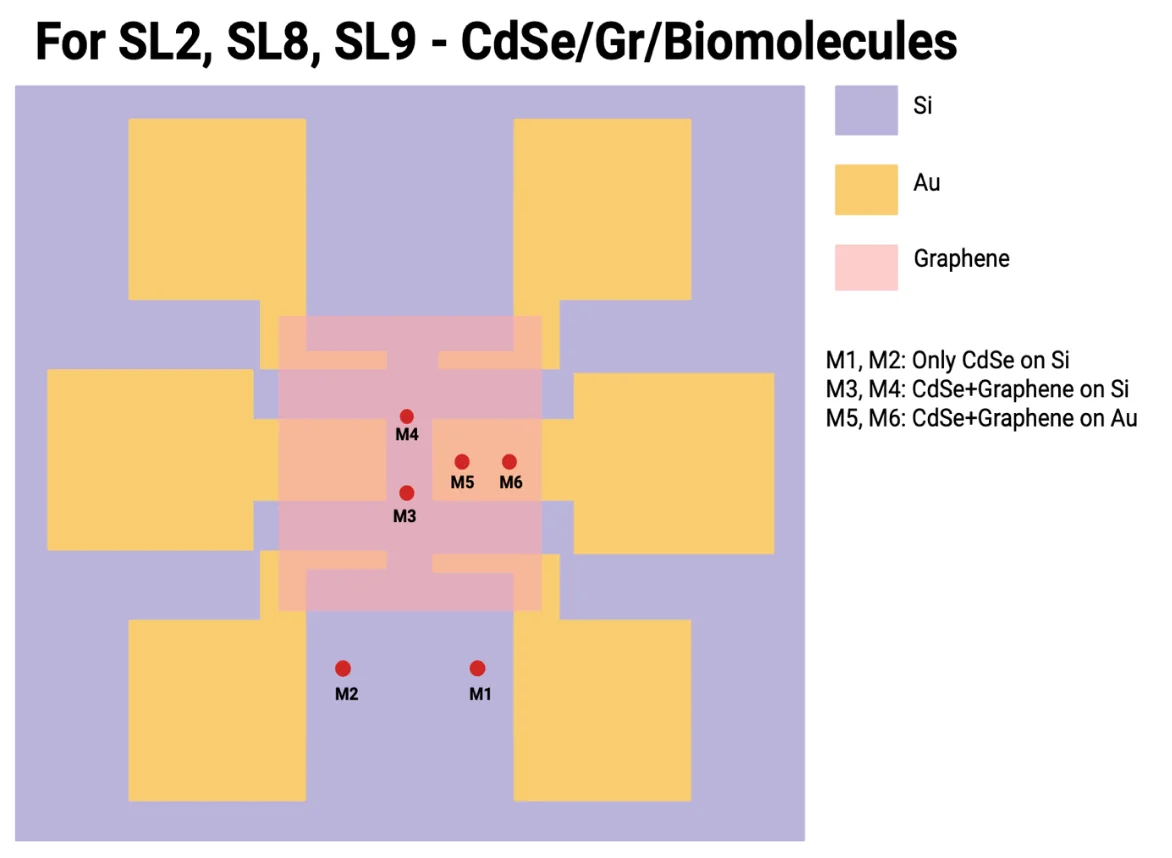
PL was measured at six locations per chip to compare emission across interfaces:
| Region | Stack |
|---|---|
| M1, M2 | CdSe only, on Si |
| M3, M4 | CdSe + graphene, on Si |
| M5, M6 | CdSe + graphene, on Au |
PL intensity by region
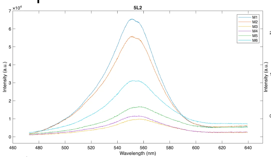
- Emission peaks near 550 nm. The CdSe-only regions (M1, M2) are brightest, while the regions with graphene (M3–M6) are markedly lower.
- This trend is consistent with graphene quenching CdSe photoluminescence.
The aptamer-based hormone biosensor I work on is written up in full on the Lal Lab page.