1. Photomask (reticle)
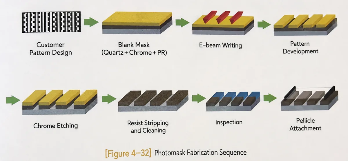
An opaque plate with a transparent pattern. Light passes through clear quartz and is blocked by chromium.
How masks are made
- Substrate prep. Ultra-flat, high-purity quartz is coated with about 100 nm of chromium and a layer of e-beam resist.
- E-beam patterning. A precision electron-beam writer draws the chip design into the resist point by point.
- Etching. The resist is developed and the exposed chromium etched away, leaving clear quartz windows. Leftover resist is removed.
- Inspection and repair. Optical or electron microscopes scan the whole mask for defects. Missing or extra chromium is fixed with focused ion beams or nanoscale lasers.
- Pellicle. A thin transparent membrane is mounted a few millimeters above the mask to keep dust off the focal plane, so particles don't print as shadows.
2. The lithography process
- Clean and prime. The wafer is treated with HMDS vapor, converting the hydrophilic Si–O–H surface to hydrophobic Si–O–Si(CH₃)₃. Photoresist is hydrophobic, so this improves adhesion.
- Spin coat. Dispense → spin up (low to high rpm) → spin off → solvent evaporation. Thickness increases with resist viscosity and decreases with spin speed. Thicker resist at the edge (edge bead) is removed by:
- Chemical EBR: a nozzle sprays solvent, often PGMEA, onto the wafer edge.
- Optical EBR: after soft bake, UV exposes only the outer 1–3 mm.
- Soft bake at 90–110 °C removes solvent, which would otherwise degrade the exposure chemistry. The resist contracts, solidifies, and bonds to the wafer. Heat also lets polymer chains relax the shear stress from spinning, evening out thickness.
- Align and expose. Laser sensors read alignment marks and adjust the stage in sub-nanometer steps until mask and wafer line up. UV or EUV light then exposes the resist through the mask. Overlay accuracy measures how well the new pattern lines up with the layers below.
- Post-exposure bake (PEB) at 110–120 °C.
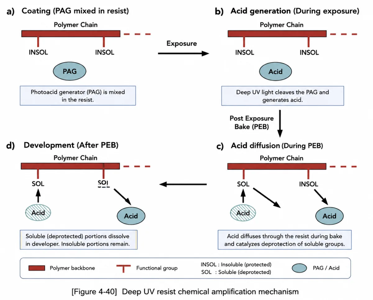
- Drives the catalytic reaction in deep-UV chemically amplified resists. Exposure alone only makes a little catalyst, and the bake's heat lets it trigger thousands of reactions.
- Smooths standing waves. Light reflecting off the substrate interferes with incoming light and leaves ripples on the resist sidewalls. Slight diffusion during PEB smooths them into straight, vertical walls.
- Develop. An alkaline developer (usually TMAH for positive resist) is applied while spinning. Development time controls how much resist dissolves. The puddle method:
- Dispense: the wafer spins at 50–100 rpm while developer is dispensed.
- Surface-tension lock: spinning stops and the developer spreads evenly.
- Static reaction: the wafer sits still while the puddle dissolves the target areas.
- Rinse and spin dry: DI water rinse, then high-speed spin to fling off liquid.
- Hard bake at 110–130 °C, above the resist's glass transition temperature but below the PAG decomposition temperature.
- Cross-links the polymer, making it more chemically inert, tougher, and heat-resistant for etching.
- Evaporates leftover water and developer that could contaminate vacuum etch chambers.
- Slightly reflows the resist to seal tightly against the wafer, rounding its top corners.
These steps all run in one track system before and after exposure. After etching or deposition, resist is stripped with O₂ plasma. With positive resist the exposed areas are removed. With negative resist the exposed areas stay.
Chemically amplified resist (CAR)
- As features shrank, lithography moved to deep-UV wavelengths: 248 nm KrF and 193 nm ArF lasers.
- DUV sources deliver far fewer photons than older mercury lamps, so standard resists weren't sensitive enough.
- Exposure: a photo-acid generator (PAG) in the resist turns into one acid molecule (H⁺) per DUV photon.
- PEB: heat activates the acid, which diffuses through the resin and catalytically turns insoluble polymer chains soluble. Because it's a catalyst, one acid molecule can repeat this 100–1000 times.
3. Photoresist
Components
- Resin: the polymer backbone.
- Solvent: keeps the resist liquid.
- Photosensitizer: changes the resin's structure when exposed. Called a PAC (photoactive compound) or PAG (photo-acid generator).
Contrast and sensitivity
- Contrast: how sharply the resist separates soluble from insoluble areas based on exposure.
- Sensitivity: how strongly the resist reacts to a given dose of light.
- Low sensitivity needs more light, which is slower.
- High sensitivity is faster but lowers resolution because of diffraction and reflection off the wafer. An anti-reflective coating (ARC) controls the reflected light.
4. UV exposure
Types of aligner
| Aligner | Gap | Trade-off |
|---|---|---|
| Contact | ~0 µm, mask touches resist | Masks wear out fast. Now mainly used in research. |
| Proximity | ~10 µm | Longer mask life, but light diffracts in the gap, lowering resolution. |
| Projection | Lenses reduce 4:1 or 5:1 | Longest mask life. The industry standard. |
Resolution
- Shorter wavelengths keep pace with smaller patterns: KrF excimer at 248 nm, ArF excimer at 193 nm, and EUV at 13.5 nm (from the 7 nm node on).
- Resolution is the minimum feature size that can be printed.
- NA (numerical aperture) is the lens system's light-gathering ability. Higher NA collects higher diffraction orders, giving sharper images.
- k₁ is a process-dependent factor (0.25–0.6) showing how optimized the process is.
- Better resolution (smaller R) comes from shorter wavelength, higher NA, or lower k₁.
- Depth of focus (DOF) is the vertical range within which the wafer surface stays in focus. A large DOF tolerates topography, wafer bow, and stage vibration.
- Higher NA improves resolution but shrinks DOF. CMP and thinner resists compensate.
R = k₁ · λ / NA NA = n · sin θ DOF = k₂ · λ / NA²
Here λ is wavelength, n the refractive index of the medium around the lens, and k₂ a process scaling factor (about 0.5).
5. Resolution enhancement techniques
From the Rayleigh equation, resolution improves by lowering k₁ or raising NA.
ArF immersion (ArFi): raising NA
- ArF excimer lasers emit deep-UV light at 193 nm.
- Immersion fills the gap between the final lens and the wafer with DI water. Water's refractive index is higher than air's, raising NA.
- Water is continuously supplied on one side and retrieved on the other, so fresh, clean water always touches the wafer. It acts like an extra lens element.
OAI, OPC, and PSM: lowering k₁
Off-axis illumination (OAI) - With on-axis illumination, light from tightly packed features diffracts at angles too wide for the lens to collect. - OAI tilts the incoming light so the 0th-order beam and one ±1st-order beam enter the lens symmetrically. Going from three beams to two lets the lens capture fine detail, improving DOF and contrast for dense, repeating patterns.
Optical proximity correction (OPC) - At sub-wavelength scales, diffraction acts as a low-pass filter: corners round, line ends shorten, and widths shift. - OPC models diffraction and resist behavior to pre-distort the mask. Serifs and hammerheads are added at corners and line ends, and sub-resolution assist features (SRAFs) placed beside isolated lines make them print like dense lines.
Phase-shift masks (PSM) - Binary chrome-on-glass masks only block light, so neighboring waves bleed together and reduce contrast. - A PSM shifts the light's phase to force destructive interference. Etching the quartz to a precise depth delays light by half a wavelength, a 180° shift. - Alternating PSM: neighboring openings alternate between 0° and 180°. The opposing waves cancel at the edge, driving intensity to zero for very sharp features. - Attenuated PSM: replaces opaque chrome with semi-transparent MoSi that shifts light 180°, creating destructive interference at feature edges without complex dual-etch mask fabrication.
6. Multiple patterning
Double exposure (LELE)
- Repeats litho–etch twice, splitting a pattern across two masks to print features twice as dense as one exposure can.
- Demands extremely precise overlay.
Self-aligned double patterning (SADP)
Doubles line density without a second alignment step. It prints one wider sacrificial line, builds sidewalls around it, then removes the center. 1. Print mandrels, the sacrificial lines. 2. Coat with a spacer film over tops, floors, and sidewalls. 3. Etch tops and floors straight down, leaving the sidewall spacers. 4. Strip the mandrels, leaving two thin lines for every original one.
SAQP (self-aligned quadruple patterning) runs SADP twice for four times the density.
7. EUV lithography
- Uses 13.5 nm light to reach sub-10 nm patterns. ArF immersion with double patterning reaches about 10 nm, and EUV needs far fewer lithography steps.
- EUV is absorbed by almost all solids, so it uses Bragg mirrors in vacuum instead of lenses.
- Still projection lithography, but the light reflects off the mask.
- Laser-produced plasma (LPP) source, vacuum operation, NA ≈ 0.33.
Light source: laser-produced plasma
- A droplet generator fires about 50,000 molten tin droplets per second across a vacuum chamber.
- A high-power CO₂ laser behind the collector hits each droplet twice.
- The tin vaporizes into ultra-hot plasma that emits 13.5 nm light in all directions through excitation and relaxation.
- A dish-shaped collector gathers the light and sends it into the optics.
Optics
- EUV is absorbed by nearly everything, including glass and air, so the whole tool runs under hard vacuum and the light bounces off mirrors instead of passing through lenses.
- Mo/Si mirrors: about 40+ pairs of reflective and spacer layers, each pair about 6–7 nm, reflect roughly 70% of the light through constructive interference (Bragg's law).
- About 70% is the maximum reflectivity per mirror, so every added mirror cuts the energy reaching the wafer and slows throughput. Mirror roughness and defects must be minimized.
Photomask
- An EUV mask is itself a mirror, with reflective and absorbing regions.
- It's an ultra-flat, low-thermal-expansion substrate coated with the same Mo/Si stack, with the circuit pattern etched into a tantalum-based absorber on top.
- Bottleneck: the pellicle that protects the mask from dust also reduces how much light the mask reflects.
Photoresist
- Each EUV photon carries high energy, but far fewer photons hit the wafer (photon shot noise), making precise line edges hard.
- Fewer photons means fewer PAG molecules activate, causing line edge roughness (LER) and line width roughness (LWR).
- Advanced nodes are moving from CAR to metal oxide resists (MOR), whose dense metal atoms, such as tin oxide, absorb EUV much better than carbon polymers.