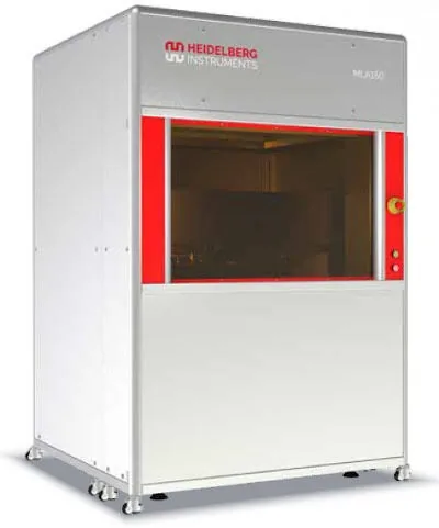
Maskless lithography
- The Heidelberg MLA writes the pattern directly from the design file, with no photomask. That makes it fast to iterate on device layouts.
- I design GFET layouts in KLayout and expose them on the MLA.
- Exposure dose runs 250–350 mJ/cm², tuned to the resist thickness.
- After exposure the wafer goes to development (see photoresist and surface profile).
For the theory behind lithography, including masks, resolution, and EUV, see my photolithography study notes.